61beplay体育
Jason Svarc
The vast majority of solar photovoltaic cells, or PV cells, are made usingsilicon crystalline wafers. The wafers can be one of two main types, monocrystalline (mono), or polycrystalline (poly) also known as multi-crystalline. The most efficient type of cell is monocrystalline which is manufactured using the well knownCzochralskiprocess. However, more recently heterojunction, or HJT cells, have become more popular due to the increasedefficiencyand improved high-temperature performance as explained in detail below.
How are silicon PV cells made?
Silicon is generally manufactured from a specific type of sand known assilica sandwhich is usually made from crushed quartz rock and contains a high percentage of a natural compound called Silica or silicon dioxide (SiO2). A number of different manufacturing processes are required to make crystalline silicon solar cells starting from the raw material quartz rock or Quartzite. First, the silica sand is converted intometallurgical grade siliconby combining Carbon and Quartzite in an arc furnace. This process occurs at very high temperatures and results in 99% pure silicon. Next, the metallurgical grade silicon is converted into Polysilicon using either a chemical purification process called theSiemens process, or upgraded metallurgical-grade silicon (UMG-Si) using a number of more economical metallurgical processes.
At this stage, the metallurgical-grade polysilicon can bedopedwith trace amounts of either boron or phosphorous to become either61beplay体育 多晶硅。多晶晶片,doped silicon is melted and cast into large rectangular blocks before being thinly sliced using a diamond wire cutter to produce thepolycrystallineormulti-crystallinewafers. The wafers can then be coated with a very thin layer of either P or N-type to form thePN-junction(photovoltaic cell).
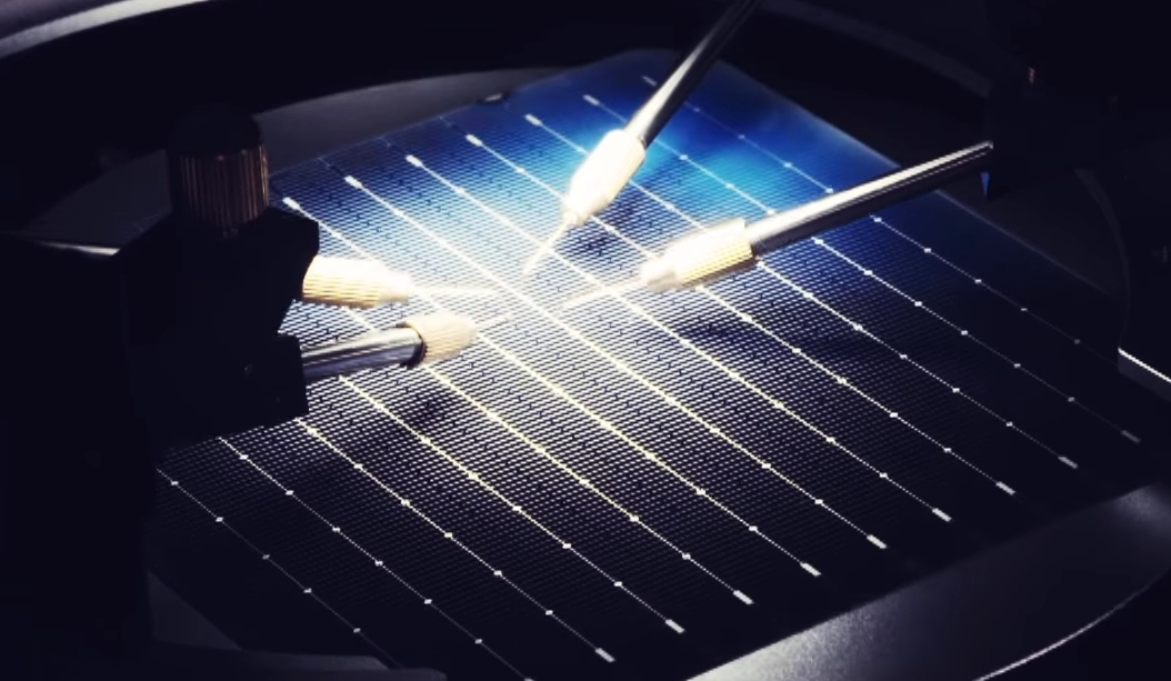
The basic materials and steps involved in making a monocrystalline solar cell - Click to enlarge
To manufacture the more efficientmonocrystallinewafers, the doped silicon can be drawn into a single solid crystal ingot using theCzochralski process. This process involves melting the polycrystalline silicon under high pressure and temperature to slowly grow a single monocrystalline crystal known as an ingot.
Basic steps to produce monocrystalline PV cells
Silica sand is purified in an arc furnace to create 99% pure silicon
The 99% silicon is further refined to become almost 100% pure silicon
The silicon is doped with either boron or phosphorous (P-type or N-type)
The doped silicon is drawn into a solid crystal ingot using theCzochralski process.
The solid round ingot is diamond wire-cut into thin square wafers
The base wafer is coated with an ultra-thin layer of either P-type or N-type silicon to form thePN-junction.
The rear side Aluminium surface field orPERClayers are added.
Metallic fingers and anti-reflective coatings are added.
Flat ribbon busbars (shown below) or thin wire (MBB) busbars are added.
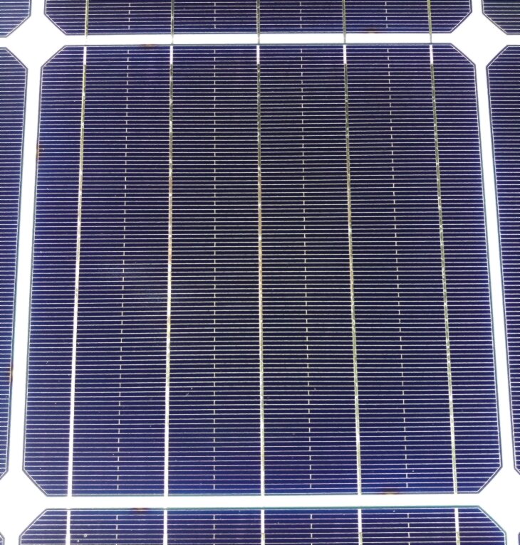
Closeup of a common monocrystalline solar cell showing the fine metallic fingers and 5 busbars.
P-Type Vs n-Type Solar Cells
All silicon crystalline solar cells are made using a very thin wafer of base silicon with the two main types being P-type and N-type. These are made when the silicon is ‘doped’ with specific chemical elements to create a positive (p-type) or negative (n-type) charge.
The chemical elements used for doping are eitherphosphorouswhich creates a positive charge andboronwhich results in a negative charge. Depending on the type of cell architecture, either N-type or P-type doped silicon is used as the base or 'substrate' of the cell. The majority of both mono and multi-crystalline cells used today use a P-type substrate that has a base of boron-doped silicon. Until recently, only a few premium manufacturers such asLG, Panasonic, SunPower,andRECused the more efficient N-type silicon wafers although many more companies are now starting to develop N-type cells as the cost is declining.N-type silicon cells are more expensive to produce but offer higher performance and a lower rate of LID orlight induced degradation, plus an improved temperature coefficient.
N-Type – Negatively charged Silicon doped with Phosphorous
P-Type – Positively charged Silicon doped with Boron
All solar cells use a combination of P-type and N-type silicon which together form thep-n junction这是基本的功能公元太阳能吗beplay全站Appll. The difference is P-type cells use the Boron doped silicon base together with an ultra-thin layer of N-type silicon, while N-type cells use an n-type silicon base with an ultra-thin layer of P-type silicon as shown in the diagram below.
P-Type Solar cells
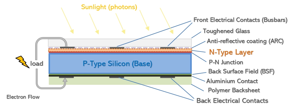
Basic construction diagram of a common P-type silicon cell
As explained above, the P-type and N-type silicon are brought together and form what’s known as ap-n junction. The junction creates an electric field which enables the flow of electrons when solar radiation passes through the cell. The photovoltaic effect is when light photons (energy) free the electrons from the silicon creating an electric current.
N-Type Solar cells
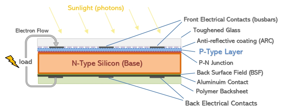
Basic construction diagram of a more efficient N-type silicon cell
Advantages of N-Type
Due to the very nature and material composition, N-type cells offer higher performance through having a greater tolerance to impurities and lower defects which increases overallefficiency. In addition, n-type cells have greater temperature tolerance compared to both mono and multi P-type cells. More importantly, n-type cells do not suffer from the issues ofLID(light-induced degradation) due to the boron-oxygen defects which are a common issue with p-type cells doped with Boron.
Lower impurities in N-type substrate
Improved high-temperature performance
Lower light-induced degradation - LID
Cost Vs Efficiency
N-type cell construction is more expensive as it uses what's known as a boron diffusion process to add the thin p-type 'emitter' layer. This diffusion process is more complex and requires higher temperatures compared to the p-type cell phosphorous diffusion process. Although N-type cells are more expensive to manufacture, the base n-type silicon is of a much higher purity which enables higher efficiency, lower losses and much lowerdegradationover time, this results in higher generation and performance which also improves payback and generally outweighs the additional upfront cost over the life of the panel.
Heterojunction Solar cells
Heterojunction or HJT solar cellsgenerally use a base of high-purity N-type crystalline silicon with additional thin-film layers of amorphous silicon on either side of the cell forming what is known as theheterojunction. The different photovoltaic materials help absorb more light photons and reduce the recombination losses thus boosting overall cell efficiency. Current HJT panels on the market such as theREC Alpha series, achieve panel efficiencies as high as 21.9%.

Basic construction diagram of a N-type Heterojunction or HJT solar cell
One of the most impressive characteristics of HJT cells is the incredibly low-temperature coefficientwhich is around 0.26%/°C. This is approximately 40% lower compared to common monocrystalline cells. Solar panel power output is rated at a cell temperature of 25°C orSTC (Standard Test Conditions), so every degree above this slightly reduces power output. In common multi and monocrystalline cells, the temperature coefficient is around 0.38% per°Cwhich can reduce total power output by up to 18% during very hot windless days. In comparison, HJT cells have a much lower temperature coefficient of around 0.26%/°Cwhich decreases cell losses down to approximately 10% on very hot days.
N-Type TOPCon Solar cells
TOPCon stands forTunnel Oxide Passivated Contactand refers to a unique rear side passivation technique first developed by the German solar research institutionFraunhofer ISEback in 2014. After five years of development, TOPCon Technology has moved into large-scale production and is expected to slowly replace the industry standard PERC cell technology over the next few years. TOPCon cell architecture essentially helps reduce what is known as therecombination losses在细胞中turn boosts cell efficiency. Due to a complex number of factors, there are several losses within a solar cell that cause electrons to recombine back into the cell without forming an electric current. TOPCon technology not only helps to reduce this recombination loss but being a full-area rear contact it also aids current flow within the cell structure and can increase cell efficiency above 25%. Note,solar panel efficiencyis always lower than the cell efficiency as it takes into account unused sections of the panel and the additional losses through all the cells, busbars and collectors.
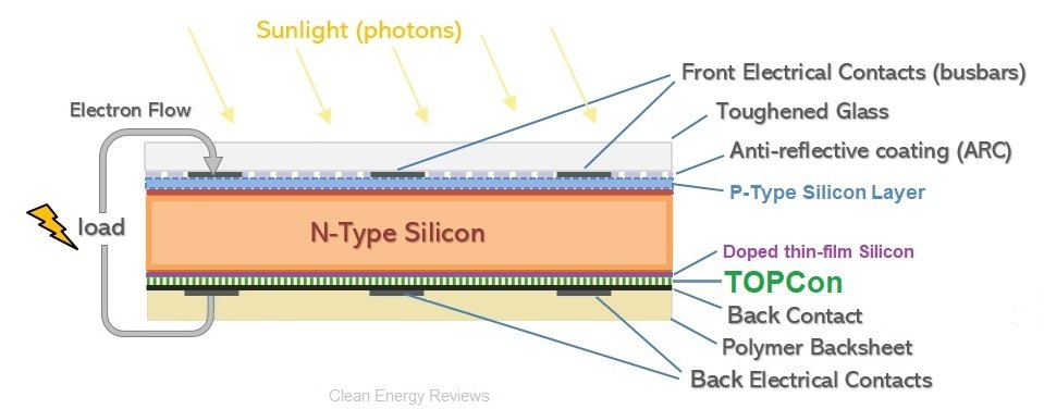
Basic construction diagram of an N-type TOPCon silicon solar cell
While TOPCon technology is generally used in conjunction with N-type substrates, it can also work effectively with more common P-type substrates to boost cell efficiency up to 24%.
Sources & References
Scientific World Journal-Advancements in N-Type Base CrystallineSilicon Solar Cells and Their Emergence in the Photovoltaic Industry - Atteq ur Rehman and Soo Hong Lee*
Electrical Engineering and Technology-www.electrical4u.com
PVeducation.org - https://www.pveducation.org/pvcdrom/pn-junctions/formation-of-a-pn-junction
https://www.aleo-solar.com/perc-cell-technology-explained/
https://www.pv-magazine.com/2021/06/02/longi-achieves-25-21-efficiency-for-topcon-solar-cell-announces-two-more-records/
How are solar panels made?
Here in ourdetailed articlewe describe how solar panels are manufactured and recycled. Solar panels are made using six main components in advanced manufacturing facilities using precise optical sensors to position each component along with specialised testing and quality control equipment.
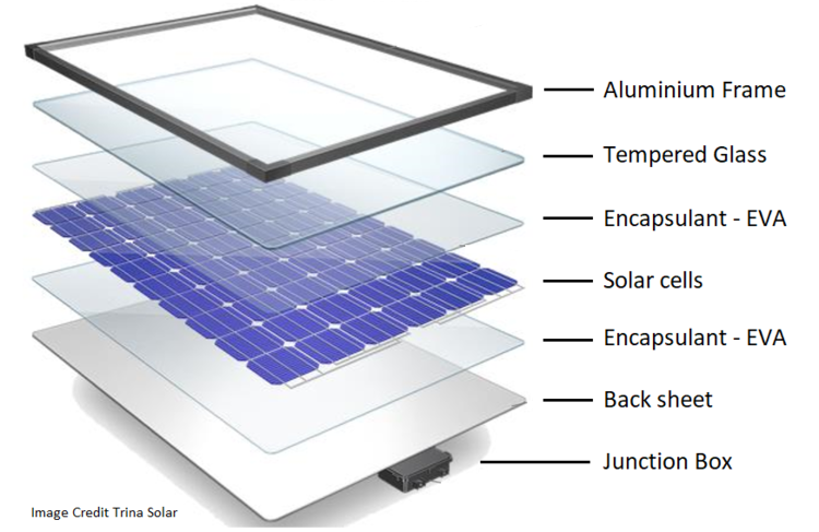
Click on the image above to go to the detailed solar panel construction article.


We review the best quality solar panels from the world’s leading manufacturers SunPower, REC, Panasonic, Q cells, Trina, Longi, and Winaico and others offering the highest performance, efficiency, best warranties and proven reliability based on independent testing by PVEL.